Author Affiliations
Abstract
1 Key Laboratory of Nanodevices and Applications, Suzhou Institute of Nano-tech and Nano-Bionics, Chinese Academy of Sciences, Suzhou 215123, China
2 School of Physical Science and Technology, ShanghaiTech University, Shanghai 201210, China
3 Shanghai Advanced Research Institute, Chinese Academy of Sciences, Shanghai 201210, China
4 University of Chinese Academy of Sciences, Beijing 100049, China
A new kind of step-flow growth mode is proposed, which adopts sidewall as step source on patterned GaN substrate. The terrace width of steps originated from the sidewall was found to change with the growth temperature and ammonia flux. The growth mechanism is explained and simulated based on step motion model. This work helps better understand the behaviors of step advancement and puts forward a method of precisely modulating atomic steps.
step-flow growth GaN terrace width step motion Journal of Semiconductors
2024, 45(2): 022501
Author Affiliations
Abstract
1 School of Nano-Tech and Nano-Bionics, University of Science and Technology of China, Hefei 230026, China
2 Suzhou Institute of Nano-Tech and Nano-Bionics, Chinese Academy of Sciences, Suzhou 215123, China
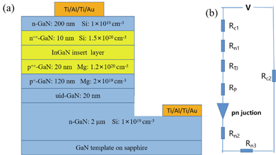
The InGaN films and GaN/InGaN/GaN tunnel junctions (TJs) were grown on GaN templates with plasma-assisted molecular beam epitaxy. As the In content increases, the quality of InGaN films grown on GaN templates decreases and the surface roughness of the samples increases. V-pits and trench defects were not found in the AFM images. p++-GaN/InGaN/n++-GaN TJs were investigated for various In content, InGaN thicknesses and doping concentration in the InGaN insert layer. The InGaN insert layer can promote good interband tunneling in GaN/InGaN/GaN TJ and significantly reduce operating voltage when doping is sufficiently high. The current density increases with increasing In content for the 3 nm InGaN insert layer, which is achieved by reducing the depletion zone width and the height of the potential barrier. At a forward current density of 500 A/cm2, the measured voltage was 4.31 V and the differential resistance was measured to be 3.75 × 10?3 Ω·cm2 for the device with a 3 nm p++-In0.35Ga0.65N insert layer. When the thickness of the In0.35Ga0.65N layer is closer to the “balanced” thickness, the TJ current density is higher. If the thickness is too high or too low, the width of the depletion zone will increase and the current density will decrease. The undoped InGaN layer has a better performance than n-type doping in the TJ. Polarization-engineered tunnel junctions can enhance the functionality and performance of electronic and optoelectronic devices.
GaN/InGaN/GaN tunnel junctions polarization-engineering molecular beam epitaxy Journal of Semiconductors
2024, 45(1): 012503
1 唐山市人民医院唐山 063000
2 河北北方学院附属第一医院张家口 075000
评价一种可降解的液态基准标志物(Liquid fiducial marker,LFM)在图像引导放疗中的应用价值。体外实验:以固态基准标志物(Solid fiducial marker,SFM)为参考,评价不同锥形束CT管电压条件下LFM的可视性、伪影和最优注量。体内实验:以SFM为参考,评价LFM在裸鼠体内的稳定性和降解状况。将种植了肿瘤细胞的裸鼠随机分为未注入LFM的单次放疗组(16 Gy/次),注入了LFM的单次(16 Gy/次)、二分次(8 Gy/次)和四分次放疗组(4 Gy/次)。根据照射结果评价LFM对肿瘤生长的影响。相比SFM,LFM的伪影显著较小(均p<0.05),可视性满足临床鉴别要求,当注量为10 μL时成像质量最佳。裸鼠体内LFM质心相对脊髓位移显著大于黄金基准标志物((0.22±0.03)mm vs.(0.17±0.02)mm,p<0.05),但始终小于一个像素尺寸,故稳定性良好。LFM的实际降解率同理论降解率高度相符。LFM对单次放疗组肿瘤生长影响较小,对分次放疗组影响较大。LFM具有一定临床应用和推广价值,未来有望取代SFM。
液态基准标志物 图像引导放疗 应用价值 Liquid fiducial marker Image guided radiotherapy Application value 辐射研究与辐射工艺学报
2023, 41(5): 050302
Author Affiliations
Abstract
1 State Key Laboratory of Artificial Microstructure and Mesoscopic Physics, School of Physics, Peking University, Beijing 100871, China
2 Frontiers Science Center for Nano-optoelectronics & Collaboration Innovation Center of Quantum Matter, Peking University, Beijing 100871, China
3 Suzhou Institute of Nano-Tech and Nano-Bionics (SINANO), Chinese Academy of Sciences, Suzhou 215123, China
4 International Center for Quantum Materials, Peking University, Beijing 100871, China
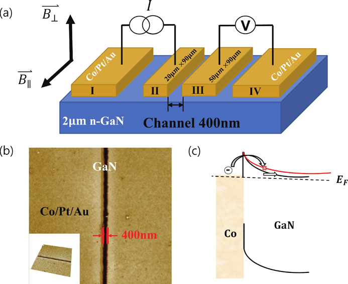
Spin injection and detection in bulk GaN were investigated by performing magnetotransport measurements at low temperatures. A non-local four-terminal lateral spin valve device was fabricated with Co/GaN Schottky contacts. The spin injection efficiency of 21% was achieved at 1.7 K. It was confirmed that the thin Schottky barrier formed between the heavily n-doped GaN and Co was conducive to the direct spin tunneling, by reducing the spin scattering relaxation through the interface states.
GaN spin injection Schottky barrier magnetoresistance Journal of Semiconductors
2023, 44(8): 082501

Siyi Huang 1,2,3Masao Ikeda 2,3,*Minglong Zhang 1,2,3Jianjun Zhu 2,3Jianping Liu 1,2,3,**
Author Affiliations
Abstract
1 School of Nano-Tech and Nano-Bionics, University of Science and Technology of China, Hefei 230026, China
2 Suzhou Institute of Nano-Tech and Nano-Bionics, Chinese Academy of Sciences, Suzhou 215123, China
3 Key Laboratory of Nanodevices and Applications, Chinese Academy of Sciences, Suzhou 215123, China
A suitable contacting scheme for p-(Al)GaN facilitating quick feedback and accurate measurements is proposed in this study. 22 nm p+-GaN followed by 2 nm p-In0.2Ga0.8N was grown on p-type layers by metal-organic chemical vapor deposition. Samples were then cut into squares after annealing and contact electrodes using In balls were put at the corners of the squares. Good linearity between all the electrodes was confirmed inI–V curves during Hall measurements even with In metal. Serval samples taken from the same wafer showed small standard deviation of ~ 4% for resistivity, Hall mobility and hole concentration. The influence of contact layer on the electrical characteristics of bulk p-type layers was then investigated by step etching technique using inductively coupled plasma etching and subsequent Hall-effect measurements. Identical values could be obtained consistently when a 28 nm non-conductive layer thickness at the surface was taken into account. Therefore, the procedures for evaluating the electrical properties of GaN-based p-type layers just using In balls proposed in this study are shown to be quick and useful as for the other conventional III–V materials.
GaN electrical properties ohmic contact Journal of Semiconductors
2023, 44(5): 052802
长沙理工大学电气与信息工程学院,湖南 长沙 410114
针对雾天图像数据集匮乏问题,提出一种基于深度估计的雾天模拟方法。自适应调整亮度与饱和度对清晰原图像进行预处理,采用自监督单目深度挖掘网络生成图像的深度图,利用引导滤波优化深度图,设定模拟图像能见度获得透射率图,通过暗通道图区分天空区域并估计大气光值,最终由大气散射模型得到设定能见度下的雾天模拟图像。实验数据显示,该方法有效改善了模拟图像目标不清晰、雾气边缘锐化问题,在模拟能见度为2000 m以下的雾天图像时效果稳定,其雾天模拟图像与真实雾天图像的特征评价指标平均误差率为6.28%,表明该方法具有可行性,可对自然环境下清晰图像进行雾天模拟以解决雾天图像数据集匮乏与能见度数据缺失的问题。
图像处理 雾天模拟 深度估计 自适应 大气光值 激光与光电子学进展
2023, 60(10): 1010005

Author Affiliations
Abstract
1 School of Nano-Tech and Nano-Bionics, University of Science and Technology of China, Hefei 230026, China
2 Suzhou Institute of Nano-Tech and Nano-Bionics, Chinese Academy of Sciences, Suzhou 215123, China
Specific contact resistance to p-GaN was measured for various structures of Ni/Pd-based metals and thin (20–30 nm thick) p-InGaN/p+-GaN contacting layers. The effects of surface chemical treatment and annealing temperature were examined. The optimal annealing temperature was determined to be 550 °C, above which the sheet resistance of the samples degraded considerably, suggesting that undesirable alloying had occurred. Pd-containing metal showed ~35% lower compared to that of single Ni. Very thin (2–3.5 nm thick) p-InGaN contacting layers grown on 20–25 nm thick p+-GaN layers exhibited one to two orders of magnitude smaller values of compared to that of p+-GaN without p-InGaN. The current density dependence of , which is indicative of nonlinearity in current-voltage relation, was also examined. The lowest achieved through this study was 4.9 × 10⁻⁵ Ω·cm2 @J = 3.4 kA/cm2.Specific contact resistance to p-GaN was measured for various structures of Ni/Pd-based metals and thin (20–30 nm thick) p-InGaN/p+-GaN contacting layers. The effects of surface chemical treatment and annealing temperature were examined. The optimal annealing temperature was determined to be 550 °C, above which the sheet resistance of the samples degraded considerably, suggesting that undesirable alloying had occurred. Pd-containing metal showed ~35% lower compared to that of single Ni. Very thin (2–3.5 nm thick) p-InGaN contacting layers grown on 20–25 nm thick p+-GaN layers exhibited one to two orders of magnitude smaller values of compared to that of p+-GaN without p-InGaN. The current density dependence of , which is indicative of nonlinearity in current-voltage relation, was also examined. The lowest achieved through this study was 4.9 × 10⁻⁵ Ω·cm2 @J = 3.4 kA/cm2.
Journal of Semiconductors
2022, 43(9): 092803
1西安应用光学研究所 国防科技工业光学一级计量站,陕西 西安 710065
为了满足高分辨率光谱仪高灵敏度、高分辨率、低噪声的技术要求,设计了用于微光成像系统的背照式CCD驱动电路及主控电路。线阵CCD采集系统采用Altera公司的MAX X系列FPGA作为核心控制器件,为线阵CCD提供多路驱动信号;线阵CCD探测器输出模拟信号经过信号预处理及AD采样,变换为数字信号后通过USB接口模块发送给光谱仪。通过将线阵CCD采集系统安装到高分辨率光谱仪,对汞灯谱线进行特征峰测试,光谱分辨率可以达到0.062 nm,满足高分辨率光谱仪的探测要求。
2西安北方光电科技防务有限公司,陕西 西安 710043
红外辐射计用于红外热像仪测试设备的校准。介绍了一种用于红外辐射计的测量模块及方法。设计了采样保持的测量方案,通过参考信号生成采样脉冲,并将采样点设置在每个信号周期的1/4相位处,能显著提高微弱信号的测量能力。对于35 ℃的黑体辐射信号,通过与现有方案的对比实验,测量信号强度可提高57.6%;在红外热像仪测试设备背景温度为22 ℃条件下,通过与现有仪器的对比测试,测量信号精度可提升50%以上。


